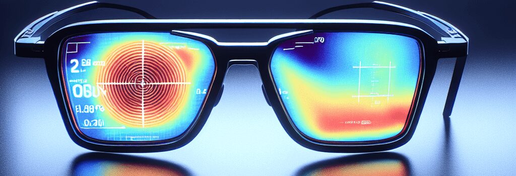
Ultra-Thin IR Films Enable Predator-Style Thermal Vision Glasses
For decades, high-end night-vision goggles have relied on bulky, liquid-nitrogen-cooled mercury cadmium telluride (MCT) focal-plane arrays to achieve high sensitivity in the mid- to long-wave infrared bands. A recent Nature paper from an MIT team introduces an alternative: wafer-scale ultrathin films of lead magnesium niobate–lead titanate (PMN-PT) just 10–30 nm thick. These pyroelectric layers operate at ambient temperature, boast a full 3–14 µm spectral response, and promise to shrink thermal-vision systems down to spectacle-frame form factors.
Fabrication Challenges in IR Detector Materials
Traditional MCT detectors achieve noise-equivalent temperature differences (NETD) below 20 mK by suppressing Johnson and phonon noise at 77 K. Cooling hardware, including cryocoolers and vacuum dewars, can add 1–2 kg per unit and consume tens of watts. Uncooled alternatives based on microbolometers or pyroelectric ceramics like tourmaline have NETDs of 50–200 mK and slower response times (100–200 µs).
Scaling down to a few nanometers introduces two major hurdles:
- Mechanical fragility: films below 50 nm tend to crack or wrinkle during liftoff.
- Interfacial adhesion: strong covalent bonds to the growth substrate prevent clean separation.
Lead Magnesium Niobate–Lead Titanate (PMN-PT): A Pyroelectric Breakthrough
PMN-PT is a relaxor ferroelectric with a high pyroelectric coefficient (p ≈ 700 µC/m²·K) and low dielectric loss. Unlike conventional piezo-pyroelectrics, its perovskite lattice tolerates tensile strain, making it ideal for direct epitaxial growth and liftoff. By incorporating lead atoms into the substrate (rather than as a release layer), the MIT group weakened the interfacial bonds and achieved sub-second mechanical peel-off of atomically smooth films without graphene or sacrificial polymer layers.
Device Architecture and Performance Metrics
The demonstrator array comprises 100 pixels, each 60 µm² in area and 10 nm thick, transferred onto a CMOS read-out integrated circuit (ROIC). Key measured parameters include:
- Spectral response: 3–14 µm (full infrared window) versus 8–12 µm for MCT.
- NETD: ~18 mK at 300 K, matching or exceeding cooled MCT detectors.
- Response time: 45 µs (improved by reducing thermal mass).
- Power consumption: <5 mW for read-out electronics, no cryocooler required.
These metrics suggest that PMN-PT devices could replace microbolometer arrays in aerial surveillance, autonomous-vehicle obstacle detection, and building-energy audits.
Scalability and Cost Analysis of the Atomic Liftoff Technique
Conventional remote epitaxy with graphene release layers can cost up to $1,000 per wafer and suffer 30–40% yield losses. By contrast, the lead-doped substrate method reduces processing steps by 50%, cuts consumables costs by 70%, and achieves >90% yield in 150 mm wafer runs. The team is now collaborating with a semiconductor foundry to adapt the process to 200 mm and 300 mm platforms using metal-organic chemical vapor deposition (MOCVD) and molecular beam epitaxy (MBE).
Comparative Analysis with Emerging 2D Material Detectors
Graphene-based bolometers, black-phosphorus photodetectors, and quantum-dot FPA prototypes have shown room-temperature responsivities of 10⁶ V/W but typically suffer narrowband operation or require complex heterostructures. PMN-PT’s advantage lies in its broadband absorption, inherent pyroelectric gain, and CMOS compatibility, simplifying back-end integration.
Potential Applications Beyond Military
While the U.S. Air Force funded the initial study, commercial sectors are poised to benefit:
- Automotive LIDAR augmentation: IR cameras with fog-penetrating capability.
- Wearable health monitors: skin temperature mapping at sub-0.1 °C precision.
- Structural inspection: real-time thermal imaging of bridges, pipelines, and solar panels.
Future Directions and Research Outlook
The MIT team plans to:
- Scale up to megapixel focal-plane arrays with 25 µm pixel pitch.
- Explore lead-free perovskites (e.g., BaTiO₃ doped with rare-earth elements) for compliance with RoHS directives.
- Integrate on flexible substrates for conformal imaging skins on drones and robots.
“Generalizing the atomic liftoff approach to various perovskites and 2D semiconductors could revolutionize how we build optoelectronic sensors,” says Xinyuan Zhang, lead author and assistant professor of materials science at MIT.
Technical Specifications at a Glance
- Film thickness: 10–30 nm ultrathin PMN-PT layers.
- Operating temperature: 20–40 °C (no active cooling).
- Spectral range: 3–14 µm full IR window.
- NETD: ~18 mK at f/1.0 aperture.
- Response time: <50 µs.
- Pixel pitch: current demo 60 µm²; target 25 µm.
- Read-out: CMOS-compatible ROIC, <5 mW per 100 × 100 array.
Expert Opinions
Dr. Sarah Lee, a senior engineer at DARPA’s Microsystems Technology Office, comments: “This ambient-temperature, broadband approach could be a game-changer for lightweight, low-power surveillance platforms. The integration simplicity is particularly impressive.”
Latest Advances and Industry Impact
In parallel, researchers at Stanford recently demonstrated a plasmonic nanoantenna array that enhances IR absorption in graphene by 10×, while a consortium led by Fraunhofer IAF is testing CMOS-backed microbolometers with sub-20 mK NETD. Combined, these efforts underscore a broader shift toward uncooled, wafer-scale IR imaging technologies.