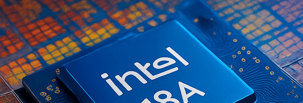
Intel’s 18A Process Faces Yield Issues Amid Roadmap Changes
By Andrew Cunningham • Updated Sep 10, 2025
Overview
Intel’s next-generation 18A node—promised to leap-frog competitors with High-NA EUV lithography and backside power rail integration—has encountered early yield difficulties, industry sources tell Reuters. With just 10% of test dies meeting performance and power specifications, Intel faces a pivotal moment in its IDM 3.0 strategy. At the same time, the company has accelerated workforce reductions, shelved European fabs, and imposed CEO sign-off on all major designs.
18A Technical Breakdown
The 18A process node was designed to implement:
- High-NA EUV (Numerical Aperture ≥0.55) to achieve sub-20 nm gate pitch.
- PowerVia Backside Power Delivery for reduced IR drop and lower metal layer congestion.
- Multi-patterned M0 and M1 Layers to optimize transistor density (~125M transistors/mm²).
- RibbonFET+2 fin-width tuning for improved drive current and leakage control.
According to an internal yield deck seen by Reuters, only 1 in 10 wafers hits leakage and frequency targets at the target voltage of 0.7 V. Intel CFO David Zinsner disputes the 10% figure—saying “yields are better”—but declined to share a precise yield rate.
Historical Context: Learning from 14A Delays
Intel’s struggles on 18A echo its 14 nm stall in 2013–2015, when delays forced Intel to extend its 14 nm line for desktop (until 2022) and mobile products. Back then, the roadmap slipped by 6–9 months as issues with 193 nm immersion multi-patterning stacks prevented consistent critical dimension (CD) control.
“We’re seeing familiar symptoms: extended tool qualification, mask overlay drift in EUV, and higher defect densities,” says Dr. Elaine Zhou, senior analyst at Semicast Research.
Latest Roadmap and External Foundry Ambitions
Despite yield concerns, Intel reaffirmed on July 30 that Panther Lake (Series 3 Core Ultra) will ship in H2 2025. Models for desktops and servers are slated for 2026. Under Pat Gelsinger’s IDM 3.0 plan, Intel is also opening 18A—and the upcoming 14A node—to external customers via Intel Foundry Services (IFS).
- IFA 2025: Intel expects to secure customer commitments before ramping 14A capacity.
- IFS Metrics: Targeting 50% utilization by 2026 with partners in telecom, HPC, and AI accelerators.
- US Govt Funding: Potential subsidy under the CHIPS Act to offset up to 30% of capital expenditure.
Business Pressures: Job Cuts and Canceled Projects
New CEO Lip-Bu Tan has imposed stringent cost controls:
- 2,400 jobs cut in Oregon in August, part of a broader 24,000 role reduction.
- Delay of the Ohio megafab ground-breaking by 6–9 months.
- Cancellation of planned fabs in Dresden (Germany) and Wroclaw (Poland).
- Spin-off of RealSense robotics/biometrics; closure of the automotive division.
“No more blank checks,” Tan wrote in an internal memo. Every project must meet ROI thresholds before funding.
Comparative Analysis with TSMC and Samsung
TSMC’s N3 (3 nm) and upcoming N2 node boast:
- ~75 nm gate pitch, ~200M transistors/mm².
- High-volume yields >50% within first 12 months.
- Strong orders from Apple, AMD, and NVIDIA AI GPUs.
Samsung’s 3GAE features backside power and EUV double patterning, yet volumes remain limited. By contrast, Intel’s aggressive timeline puts it 12–18 months behind TSMC’s ramp.
Impact on the Global Fab Ecosystem
Analysts warn that further delays or cancellations at Intel could:
- Reduce US-based foundry capacity, increasing dependence on Taiwan and South Korea.
- Drive OEMs to hedge with multi-sourcing strategies, adding inventory buffers.
- Slow adoption of emerging packaging technologies (e.g., Foveros, EMIB) if underlying nodes are unstable.
Outlook for Intel Foundry Services (IFS)
IFS was pitched as a key pillar of IDM 3.0, aiming to capture 15–20% of the global foundry market by 2028. Success depends on:
- Customer Trust: Convincing fabless companies to commit to 14A/18A despite yield PR risks.
- Government Incentives: Leveraging CHIPS Act grants to underwrite expansion.
- Execution: Meeting ramp milestones for EUV tool installs, defect density targets (<1 cm² DPPM), and CD uniformity (±2 nm).
Expert Opinions
“Intel’s technological roadmap is impressive on paper—High-NA EUV and backside power are industry firsts—but execution will make or break its foundry credibility.” — Dr. Michael Wang, semiconductor consultant
“With global fab capacity tight through 2026, there’s room for IFS if Intel can stabilize yields and secure anchor customers.” — Jane Lee, VP of Market Strategy at ChipInsights
Conclusion
Intel’s 18A process stands at a crossroads: it must overcome early yield challenges while navigating steep cost cuts and strategic realignments. The next two quarters will be critical—Panther Lake’s tape-out, the Ohio fab’s ground-breaking, and IFS customer wins will determine if Intel can reclaim foundry leadership or cede ground to TSMC and Samsung.